
TL;DR
- An annular ring is the band of copper left around a drilled hole, between the hole edge and the outer edge of the pad. Ring width = (pad diameter − finished hole diameter) ÷ 2.
- A common design-for-manufacture floor is 6 mil (0.15 mm) of ring. IPC-2221 specifies a minimum land of roughly 0.05 mm per side for a plated hole, and IPC-6012 grades what a fab must ship by class.
- Rings break in two ways: tangency (the hole touches the pad edge, zero ring at one point) and breakout (the hole punches through the pad). Both come from drill wander and layer misregistration.
- Class 2 boards tolerate limited breakout on inner layers; Class 3 boards allow none and require a larger ring.
- Teardrops are the cheapest fix: they add copper exactly where the breakout starts. Turn them on before you export Gerber files.
An annular ring is the ring of copper that remains around a drilled hole once the drill passes through the center of its pad. Annular ring width on each side is given as: (pad diameter − finished hole diameter) ÷ 2. Yes, it is trivial! But it is the single most common reason why a design passes DRC on your screen and then comes back from the fab flagged for “insufficient annular ring” or worse, it failed continuity after thermal cycling.
This ring electrically and mechanically ties the plated barrel of a hole to the copper trace on the PCB surface. And if you squeeze it too thin, the connection lives on the edge of the fab’s capabilities. This guide covers what the annular ring is, how to size it, what the standards actually require, why it fails, and the checks that you should perform before your Gerbers leave your desk.
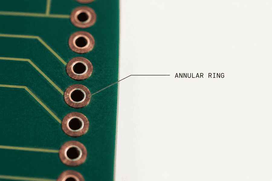
What Is an Annular Ring?
An annular ring is the copper left between a drilled hole and the outer edge of its pad. Imagine a copper pad with a perfectly centered drilled hole. The remaining ring of copper surrounding that hole is the annular ring. In a plated hole, the copper doesn’t stop at the surface; it continues down the hole to form the plated barrel. The annular ring is the copper landing zone where the surface pad joins the barrel inside the PCB.
Every plated through-hole, via, and component pad has one. Its job is simple but load-bearing: give the drilled-and-plated hole enough copper to hold onto, so the joint survives drill misalignment and years of thermal expansion. Think of the annular ring as a safety margin around the hole. When the ring is healthy, minor drilling variations don’t matter. When it is marginal, a fraction of a millimeter of drill drift can turn a perfectly good PCB into a scrap panel.
The annular ring is determined by just two dimensions: the pad diameter and the finished hole diameter. The catch is that the hole used in the calculation is the finished hole, not the drill bit size. Since plating reduces the hole diameter, using the raw drill size can lead to incorrect annular ring calculations.
Annular Ring Anatomy: Pad, Drill and Ring Width
The geometry is a set of concentric circles. Outermost is the copper pad (the “land”). Inside that is the drilled hole. After plating, copper is deposited on the barrel wall, which shrinks the opening, so the finished hole is smaller than the drill that made it. Plating typically accounts for about 0.1 mm of the drill diameter, though the exact figure depends on your fab’s plating spec. Treat it as a rule of thumb and confirm the number from the manufacturer’s capabilities section.
That distinction matters for where you measure. On outer layers, the ring is measured from the finished (plated) hole to the pad edge. On inner layers, it is measured from the drill diameter to the pad edge, because the inner copper is exposed to the drill, not the plated barrel. The same board has two reference points, and it is obvious to have confusion when a fab report and your CAD tool disagree by a hair.
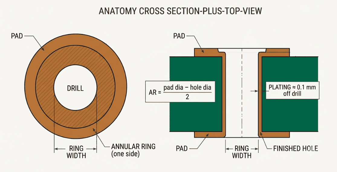
The width formula is straightforward: AR = (pad diameter − hole diameter) ÷ 2
You divide by two because the ring exists on both sides of the hole; the formula gives the width of copper on a single side, which is the number the standards and your DRC actually check.
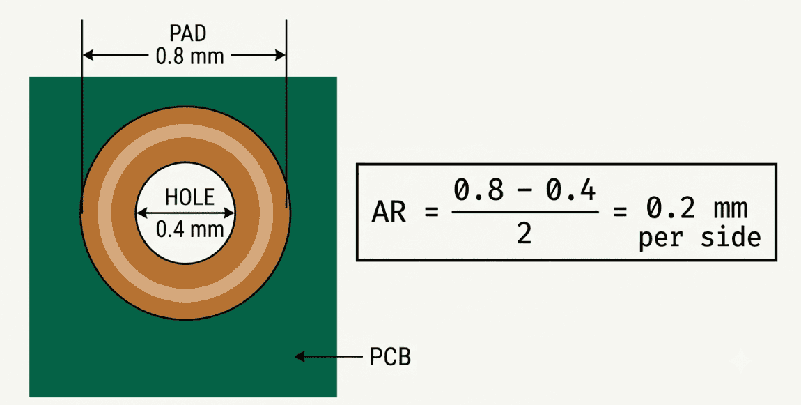
Worked example for Annular Ring (AR) width:
Take a common through-hole pad:
- Given: pad diameter = 0.8 mm, finished hole = 0.4 mm
- AR = (0.8 − 0.4) ÷ 2
- AR = 0.4 ÷ 2 = 0.2 mm per side
That 0.2 mm (about 8 mil) is a comfortable ring that exceeds the typical 6 mil fabrication minimum spec, providing additional tolerance for drill misregistration. Now watch what happens if you specify a 0.8 mm pad against a 0.5 mm drill that plates down to a 0.4 mm finished hole: on the outer layer, you still get 0.2 mm. But the inner-layer annular ring is only 0.15 mm, because the inner copper is drilled before plating and therefore references the drill diameter, not the finished hole. The result is simple: the inner layer is almost always the critical case. So, size it according to the inner dimensions.
Minimum Annular Ring: What the Standards Say
There is no single magic number — it depends on which reliability class your board is built to. IPC-6012 is the performance spec for rigid boards, and it sorts requirements into three classes:
| Class | Typical use | Annular ring expectation (plain language) |
|---|---|---|
| Class 1 | General consumer | Breakout tolerated fairly liberally |
| Class 2 | Dedicated service electronics (most commercial products) | Some breakouts allowed, but a substantial arc of the ring must stay intact. |
| Class 3 | High-reliability (aerospace, medical, life-support) | No breakout permitted; a minimum ring must remain at every point, driving tighter drilling and registration |
Design with margin. Because drill wander, image registration, material movement in lamination, and plating variation all eat into the ring, you want the as-drawn ring comfortably above the fab acceptance floor. A 6 mil (0.15 mm) minimum ring is a widely used general-purpose target that leaves the fab room to hit spec. High-density boards go lower, but only after you have confirmed your manufacturer’s capability. Every fab publishes its own annular-ring minimums; check the current rules before you commit, because they vary with layer count, technology, and equipment.
Tangency and Breakout: How Rings Fail
A ring fails when the hole ends up somewhere other than the center of the pad. Two things push it there: drill wander (the bit drifts off the programmed position) and layer misregistration (the drilled stack doesn’t line up perfectly with the imaged copper).
There are three states worth naming:
- Full ring — the healthy case; copper surrounds the hole on all sides with margin to spare.
- Tangency — the hole edge just touches the pad edge. The ring is zero at one point. Some classes accept it, but class 3 does not.
- Breakout — the hole punches past the pad edge, and copper is missing over an arc. The trace-to-barrel connection now depends on whatever copper is left.
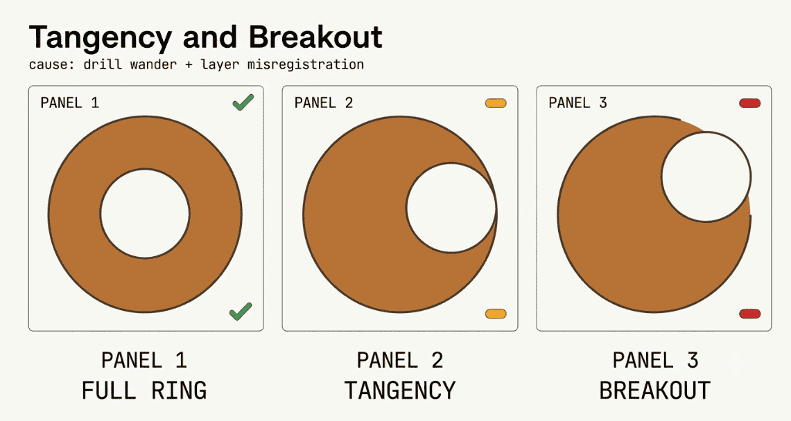
This is exactly why the classes differ. Class 2 tolerates some breakout due to a partial ring and sufficient copper over a sufficient portion of the circumference. Class 3 forbids it because a life-support board can’t gamble on the one via that lost its collar.
Teardrops: cheap insurance
A teardrop is a small fillet of copper added where a trace meets a pad or via. It flares the connection outward like a drop of water, so the junction has more copper exactly where the breakout is most likely to start. When the drill drifts toward the trace side, that extra copper keeps the connection intact instead of leaving a thin neck.
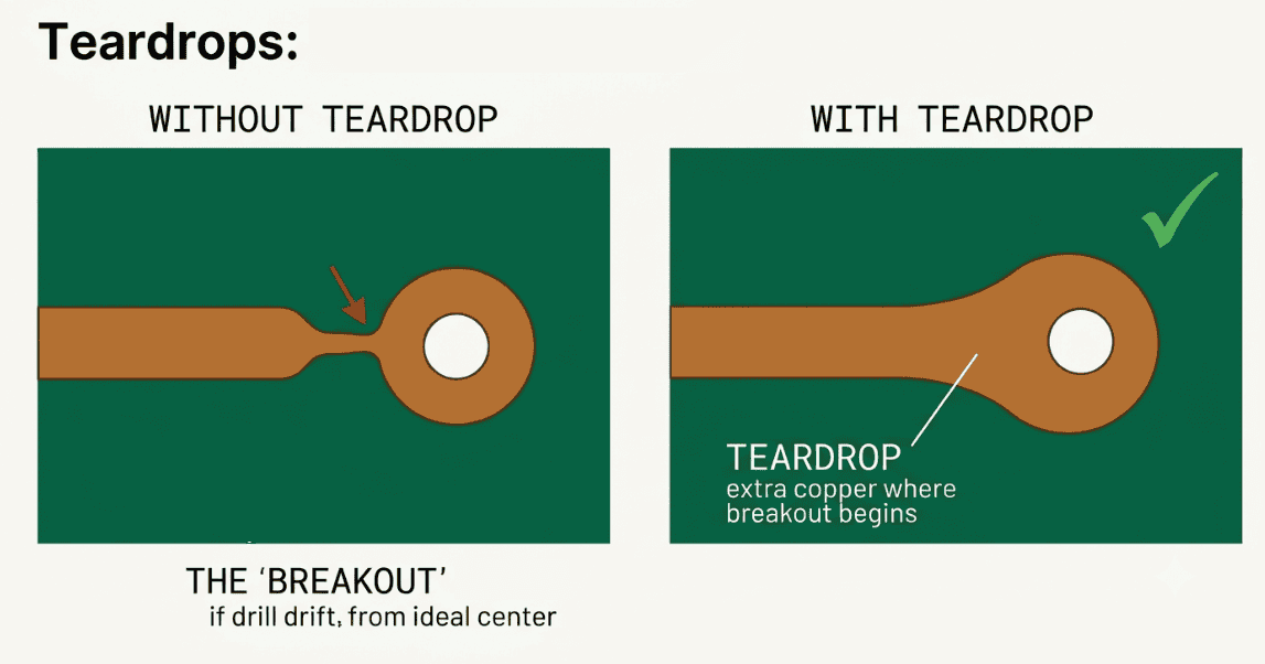
Teardrops cost you nothing in fabrication, and most fabs will happily add them; many will even apply them automatically at CAM if you ask. In your CAD tool, teardrops are usually a one-click design rule. Enable them for pads and vias, set the size, and let the tool fill them in before Gerber export. On tightly packed boards, teardrops add cheap insurance. If your PCB design software supports teardrops, it’s generally worth enabling them as part of your standard DFM workflow.
Annular Ring Rules for Vias and Component Holes
Not every hole needs the same ring, because they do different jobs.
Vias exist only to carry a signal or power between layers, so there is no mechanical load, no solder joint, no component lead. That lets them tolerate a smaller ring, since you’re only protecting the barrel-to-trace connection. On space-constrained boards, shrinking via rings is one of the first levers you pull to route more densely.
Component holes contain through-hole leads. Beyond the electrical connection, the ring has to support a solder fillet, so plated through-hole pads generally carry more copper than a signal via.
A note on annular rings in microvias: laser-drilled microvias play by different rules. A laser places a hole with far tighter accuracy than a mechanical drill. It is of the order of under 2 mil, which leaves roughly 3 mil for mechanical drilling, so microvias run with much smaller rings, often as via-in-pad.
CAD Checklist Before Gerber Export
Most annular-ring problems are caught in thirty seconds if you run the right checks before you generate manufacturing files:
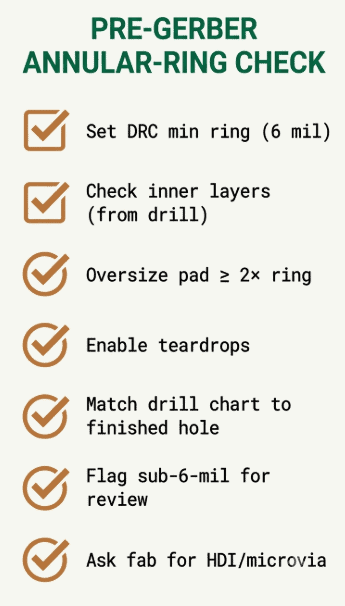
- Set your DRC minimum annular ring to your target: 6 mil is a safe, general default.
- Check inner-layer rings separately. Remember they’re measured from the drill, not the finished hole.
- Oversize pads relative to drills: pad diameter should exceed the finished hole by at least twice your target ring (e.g., a 0.8 mm pad for a 0.4 mm hole gives 0.2 mm per side).
- Enable teardrops on pads and vias, then re-run DRC. They cost nothing and buy real margin.
- Flag anything below the general floor for review. If a ring has to go below 6 mil for routing density, that’s fine, but it becomes a conversation with your fab.
- Ask the fab when in doubt. For HDI, microvias, or high-layer-count boards, pull their current annular-ring capabilities and design accordingly, not to a generic number.
Keep this as a standing pre-export ritual. It’s the difference between a clean fab review and a back-and-forth that delays your build. If you want a printable version, save these six steps as a one-page DFM check and pin it next to your other pre-Gerber rules.
FAQ
Q. What is an annular ring in a PCB?
Ans. It’s the ring of copper left around the drilled hole, between the hole’s edge and the pad’s outer edge. On a plated hole, it bonds the surface pad to the plated barrel, giving the connection enough copper to survive drill misalignment and thermal stress.
Q. How do you calculate annular ring width?
Ans. Use the formula (pad diameter − finished hole diameter) ÷ 2. For example, a 0.8 mm pad with a 0.4 mm finished hole gives (0.8 − 0.4) ÷ 2 = 0.2 mm of ring per side.
Q. What is the minimum annular ring per IPC?
Ans. It depends on the class. IPC-6012 sets acceptance floors at about 0.05 mm (about 2 mil) of remaining copper for Class 3 external layers. IPC-2221 frames a plated hole’s minimum land around 0.05–0.1 mm per side.
Q. What causes an annular ring breakout?
Ans. A breakout occurs when the drilled hole is off-center enough that it punches past the pad edge, leaving copper missing over part of the ring. The two culprits are drill wander (the bit drifting off position) and layer misregistration (the drilled stack not aligning with the imaged copper).
Q. What is tangency in PCB drilling?
Ans. Tangency is the state where the hole edge just touches the pad edge, so the annular ring is zero at exactly one point. It sits between a full ring and a full breakout. Some reliability classes accept it, especially with teardrops added.
Q. Do teardrops prevent annular ring failure?
Ans. Teardrops add copper where a trace meets a pad, exactly where breakout is most likely to begin, so they meaningfully reduce the risk of a broken connection.
The Bottom Line
An annular ring is a tolerance budget disguised as a geometry rule. The formula is trivial; the discipline is in leaving enough copper that normal drill wander and registration drift can happen without eating your connection. Design to a comfortable ring like 6 mil, size to your inner layers, turn on teardrops, and treat any sub-floor ring as a deliberate conversation with your manufacturer.
If you found this guide helpful, you’ll probably enjoy our other PCB design resources. We publish practical, engineer-written articles covering topics such as standard PCB thickness, PCB vs. PCBA, through-hole vs. SMD components, and SMD package sizes.
If you’re building hardware and need technically accurate content for your company, we also create engineering blogs, application notes, and educational resources written by working PCB engineers.
Our goal is to help electronics companies publish content that engineers actually trust and search engines reward. Want to see the difference engineer-written content can make? Start with a free pilot article of up to 1,200 words, tailored to your website and written by working PCB engineers. More about how we work: services & pricing.